Key Takeaways
A team of university researchers recently demonstrated that passive, battery-free wireless strain sensors can be fully 3D printed in a single build process, using direct-write multi-material additive manufacturing with nano3Dprint’s systems. Engineers co-print flexible polymer substrates with conductive silver antenna patterns for real-time structural health monitoring (SHM).
What are 3D Printed Passive Wireless Strain Sensors?
A 3D printed passive wireless strain sensor is a battery-free electronic component designed to monitor physical stress and deformation in civil, aerospace, and mechanical structures.
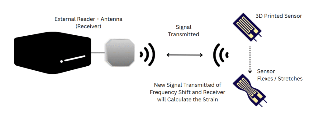
Instead of relying on internal batteries or complex wiring, the sensor functions as a Radio Frequency (RF) patch antenna. When the underlying structure stretches or bends, the geometry of the 3D printed conductive antenna changes. An external reader detects this shift in resonant frequency to calculate exact structural strain in real-time.
How the nano3Dprint’s Additive Manufacturing Systems Enables Multi-Material Sensor Fabrication
Traditional sensor manufacturing requires separate steps for molding substrates, lithography, and manual adhesive assembly. With nano3Dprint’s systems, it simplifies this into a single step through multi-material direct-write technology.
Key Print Process Steps on the nano3Dprint MatDep Pro:
- Substrate Deposition: The nano3Dprint MatDep Pro extrudes a flexible polymer layer (such as TPU or PLA) to form the structural base of the sensor.
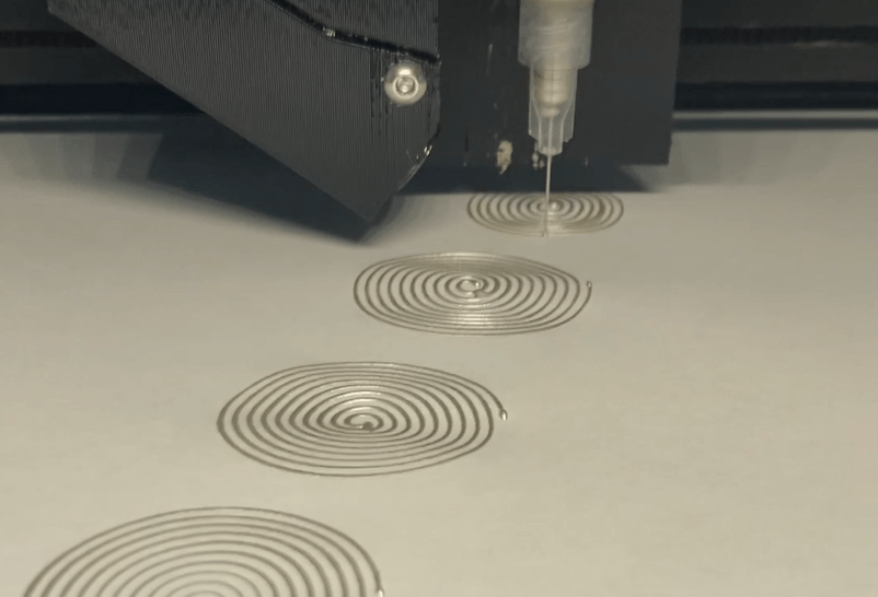
- Direct-Write Conductive Tracing: Using its high-precision liquid/paste dispensing head, the MatDep Pro deposits conductive silver nanoparticle ink directly onto the substrate to construct the high-frequency antenna shape.
- Encapsulation: A protective polymer top layer is then printed over the silver traces, sealing the conductive antenna against moisture and mechanical wear.
Why Choose nano3Dprint Hybrid Additive Manufacturing Systems for Printed Electronics R&D?
nano3Dprint has specifically designed their systems for functional electronics, bio-printing, and smart materials research.
| Feature / Capability | nano3Dprint Advantage for Sensor Fabrication |
| Multi-Material Dispensing | Combines standard FDM filaments with liquid inks, functional pastes, and hydrogels in one print. |
| High-Viscosity Ink Compatibility | Handles conductive silver, carbon nanotubes (CNT), copper oxide, and bio-inks without clogging. |
| Open Material Compatibility | Don’t get locked into a single ink type or proprietary ink. Feel free to utilize third-party inks or specialized inks. |
| Direct-Write Precision | Delivers fine trace resolution needed for RF antennas, capacitors, and micro-sensors. |
| Limited to No Manual Assembly | Eliminates conductive adhesives and wire alignment by printing both active and passive layers. |
Frequently Asked Questions
Can the nano3Dprint MatDep Pro print conductive silver inks? What about the nano3Dprint A2200 or the nano3Dprint B3300?
Yes. All of nano3Dprint’s systems can print conductive silver inks. The nano3Dprint MatDep Pro and the nano3Dprint A2200 features the high-precision syringe dispenser module capable of extruding high-viscosity conductive silver nanoparticle inks, metallic pastes, and functional liquid polymers alongside standard FDM filaments. While the nano3Dprint B3300 features two high-precision syringe dispenser modules side-by-side (no FDM capability).
What applications can be created with the nano3Dprint MatDep Pro? What about the nano3Dprint A2200 or the nano3Dprint B3300?
nano3Dprint MatDep Pro, A2200, and B3300 are used across academic and industrial R&D for applications including:
- Passive wireless strain and environmental sensors
- Flexible wearable electronics and smart textiles
- Micro-supercapacitors and energy storage devices
- Embedded circuit passives (capacitors, inductors, resistors)
- Piezoresistive force transducers and tactile skins
How can I prevent layer delamination when using the nano3Dprint MatDep Pro? What about for the nano3Dprint A2200 or the nano3Dprint B3300?
Delamination typically occurs due to rapid thermal contraction, poor interlayer adhesion, or stresses caused by combining standard FDM thermoplastics with functional electronic inks/pastes. To prevent delamination on the MatDep Pro and prolong the lifespan of the printed part, follow these best practices:
- Match Inks and Substrates: Choose the appropriate ink or paste specifically formulated for your substrate material. Ensuring chemical and thermal compatibility guarantees that the functional ink or paste properly adheres to the underlying substrate, preventing premature peeling or separation.
- Optimize Print Temperatures: Ensure your FDM nozzle and heated bed (which reaches up to 120°C are set to manufacturer-recommended ranges for materials like TPU, ABS, Nylon, or PC. Insufficient extrusion or low print temperatures weaken inter-layer bonding.
- Manage Ambient Environment: Minimize drafts and ambient temperature fluctuations around the build volume to prevent the upper layers of shrink-sensitive thermoplastics from cooling too quickly.
- Control Dispensing Interlayer Timing: When embedding conductive inks or dielectric pastes within structural FDM layers, ensure that wet or solvent-based pastes have appropriate drying or curing intervals. Trapped solvents or uneven layer heights from the Materials Dispensing System can create structural gaps that disrupt subsequent FDM bonding passes.
- Utilize Protective Encapsulation: Prevent peeling and mechanical separation at multi-material interfaces by encapsulating the functional inks and pastes. You can apply a protective polymer top layer, a silicone top layer, or an acrylic top layer using the dispensing system to seal the embedded traces and structurally lock the layers together.
- Utilize Real-Time Monitoring: Leverage the built-in video inspection system to closely monitor multi-material integration layers as they print, ensuring consistent material deposition without gaps or misalignment.
These best practices also apply to the nano3Dprint A2200 and the nano3Dprint B3300.
Where can I buy or learn more about nano3Dprint products?
You can explore detailed technical specifications or consult with the technical team directly on nano3Dprint Contact Page, by email info@nano3Dprint.com, or the product pages:
If you are interested in applying these techniques with robotics, contact our Robotics Division.