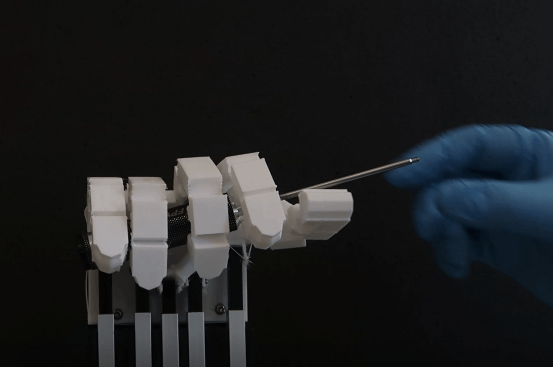
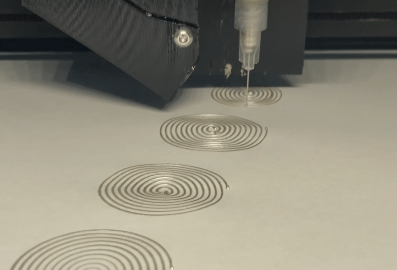
Nano3Dprint is a 3D printer provider which specializes in combining two previously unrelated fields. Our goal is to democratize inventorship within this developing industry so that private, non-corporately funded individuals can have the opportunity to research and develop their own designs. Couple that mission with our innovative printable electronics-based 3D printers, which have the functionality to print at both the micro levels, and you begin to understand what makes us such a unique business
But what does that mean, exactly? Well, we are glad you asked. And because our readers have a variety of levels of understanding regarding this topic, we will take a look at a specific application which many of our customers have an interest in – printed circuit boards, or PCB for short. Read on if you are interested in how printed circuit boards are useful in the modern era, along with Nano3Dprint’s role in affording people like you the opportunity to reach out and be a part of the world of printed electronics.
Let’s Start With The Basics
The beginning is a very good place to start, as Julie Andrews taught us all from a young age. PCBs can also be called printed wiring boards or, to some uncivilized barbarians, “printed wiring cards”. But to each their own, we suppose.
Before one could print a circuit board, complex circuit boards had to be arduously assembled by hand. The drawbacks to such a method are fairly obvious, but chief among them were simple human error combined with short circuits when wire insulation cracked due to environmental exposure and time.
As time wore on, our methods for prolonging functionality improved. Wire wrapping was one such technique which bore the fruit of sustainability. This was a method where a tiny gauge is wrapped around a post at each point of connection, which made a more durable connection.
PCB Arrives
On to the scene comes printed circuit boards. A PCB is characterized by having pads and lines which connect points, connectors, and components to one another. A PCB lets signals transfer between physical devices on the board.
The composition of a PCB, like all 3D printed objects, is layered. But PCBs are unique in that they have a substrate, copper, soldermask, and silkscreen. Let’s take a closer look at what each component contributes:
- Substrate – Also referred to as an FR4, this is the base layer of the PCB. It is usually fiberglass in material, and can vary in thickness, depending on the intended use. While some substrates are less expensive than fiberglass (like phelonics or epoxies), you get what you pay for in this instance. Phelonics, for example, have a much lower thermal decomposition temperature which means they are more prone to failure down the road.
- Copper – Next up is a copper foil, which must be adhered to the board with heat. It is not uncommon to see a copper layer applied to both sides of the substrate. A typical PCB will have one ounce of copper per square foot of actual board.
- Soldermask – Over the top of the copper layer comes the layer of soldermask. This insulates the copper from environmental exposure, which means less potential error in terms of solder jumpers and the like.
- Silkscreen – The final component of the circuit board discussed today. On top of the soldermask layer comes the white silkscreen layer. This is used for symbols, words, and letters in order indicate function and direction.
Print Your Own Circuit Board
Now, that you understand the basics of PCBs, you are probably ready to print your own! Just kidding, there is much, much more that goes into this process than what we have discussed today.
But, luckily, you have a great resource in us at Nano3Dprint, where we do much more than sell people affordable, pioneering printers. We are here to consult with you on your project, help you brainstorm or fill in the missing pieces, or even print your completed design for you!
But before we go that route, here are a few general tips you need to get started on designing your own PCB.
- Get a CAD file package. There are plenty of free options out there for you to choose from. You’ll want to consider what kind of community resources and support exist for your selected package, because the odds are that you will encounter more than a few bumps in the road.
- Open source hardware is worth consideration, as it is always being improved.
Consider Nano3DPrint
The bottom line is that however little knowledge you had before you read this article, you can walk away with one concrete piece of information. And that is that Nano3Dprint is a fantastic resource for printable electronics, printable circuit board assistance, and any other questions you might have in this area. Whether you have all the working knowledge you need and are simply looking for a great printer to bring your PCB to life, or are in need of consultative services, Nano3Dprint represents incredible value for the services we provide. Reach out to us today for more information on PCB printers, conductive graphene filament, and printable electronics.